Eseandre Mordi
TSMC just made a bold move in the global AI hardware race, pushing its next-generation packaging timeline way ahead of schedule. This matters because competition around manufacturing bottlenecks is getting fiercer, and the world's supply of AI accelerators is still limited by production constraints. TSMC's accelerated CoPoS roadmap is one of the biggest strategic shifts in semiconductor packaging we've seen in years.
310mm Panels Coming by 2028
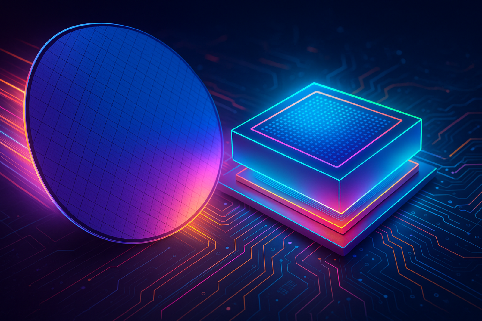
Taiwan Semiconductor Manufacturing Co. is moving forward with its CoPoS (Chip-on-Panel-on-Substrate) technology, switching from wafers to large 310mm × 310mm packaging panels to handle the massive surge in demand for AI GPUs and custom silicon.
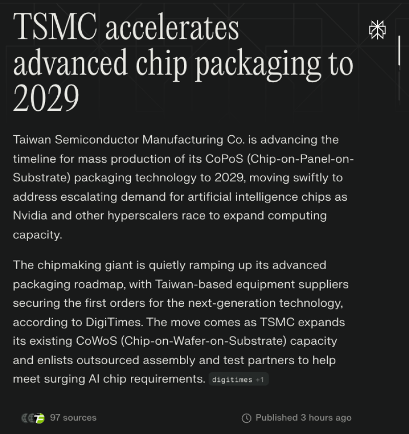
The company will launch a pilot line at VisEra in 2026, then ramp up to full mass production at its Chiayi AP7 plant between 2028 and 2029. Nvidia is widely expected to be among the first customers lining up for this upgraded packaging capability.
Why CoPoS Matters for AI Chips
TSMC's decision to speed up CoPoS reflects just how fast AI computing is growing worldwide. Traditional packaging platforms like CoWoS (Chip-on-Wafer-on-Substrate) are already maxed out, and advanced AI chips — especially high-bandwidth GPU modules and custom accelerators — need new packaging formats that deliver higher density, better thermal performance, and way more throughput. By switching to panel-based packaging, TSMC dramatically expands usable area per unit, clearing bottlenecks and making it much easier to scale production of large-footprint AI components.
Industry Ramp-Up Already Underway
Industry reports show TSMC is simultaneously expanding its CoWoS capacity while working with Taiwan-based equipment suppliers who've already secured the first orders for next-generation packaging tools.

This steady ramp-up signals that customer demand — driven by hyperscalers and AI chip designers — is climbing faster than anyone expected. The move from wafers to rectangular panels isn't just about manufacturing efficiency; it's a fundamental change in how the semiconductor industry will build future AI hardware.
What This Means for AI's Future
TSMC's accelerated CoPoS timeline matters because it will directly impact the availability, competitiveness, and scalability of the next wave of AI chips. As AI workloads keep pushing silicon to its limits, packaging has become one of the major constraints on global compute capacity. By bringing panel-based production forward to 2028-2029, TSMC is positioning itself at the center of the next decade of AI hardware innovation — where packaging, not lithography, might be what determines who leads the world in compute performance.
 Eseandre Mordi