Peter Smith
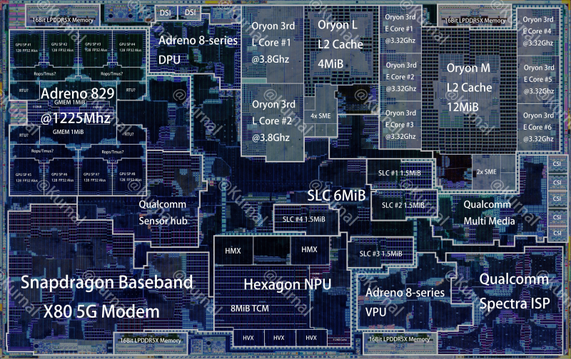
⬤ A detailed die shot of the Qualcomm Snapdragon 8 Gen5 (SM8845) has surfaced, giving one of the clearest looks yet at the flagship mobile processor's internal layout. The chip measures 12.8mm by 8.09mm, totaling 103.552mm². The annotated image breaks down the major components including the Adreno 8-series GPU, Oryon CPU clusters, Hexagon NPU, Snapdragon X80 5G modem, Spectra ISP, and shared system cache. Chip analysts are taking a close look at how Qualcomm has arranged these components and what it means for smartphone performance.
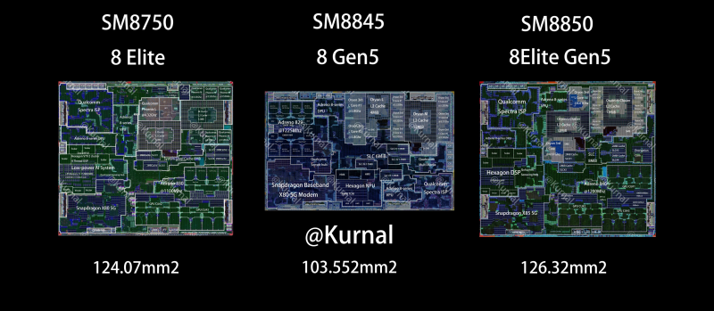
⬤ The comparison images stack the Snapdragon 8 Gen5 against the Snapdragon 8 Elite (SM8750) and Snapdragon 8 Elite Gen5 (SM8850). The SM8750 measures 124.07mm², the SM8845 comes in at 103.552mm², and the SM8850 hits 126.32mm². That makes the Snapdragon 8 Gen5 noticeably smaller than both Elite variants, yet it still manages to pack in high-performance CPU and GPU blocks, the integrated Snapdragon X80 5G modem, and the Hexagon NPU. Market watchers are keeping an eye on how Qualcomm balances chip size with AI processing power and energy efficiency.
⬤ The die map highlights Oryon performance and efficiency CPU cores, multi-megabyte L2 and system caches, Adreno graphics cores, and the Spectra ISP for camera processing. The Hexagon NPU and dedicated AI components show Qualcomm's approach of spreading intelligence across the CPU, GPU, and neural engines. The Snapdragon 8 Gen5 is being positioned as a flagship platform, and these layout details offer a rare glimpse into how the company is organizing compute, connectivity, and multimedia capabilities on a single chip.

⬤ Die size and component placement matter because they directly impact performance, power draw, heat management, and what devices can actually do. As AI workloads, graphics demands, and wireless connectivity needs keep growing, the design decisions Qualcomm makes shape how competitive Android flagships can be, what they cost to produce, and how quickly new features reach the market.
 Peter Smith