Victoria Bazir

⬤ Samsung Electronics, SK Hynix, and Micron are locked in a high-stakes race to develop 16-HI High Bandwidth Memory after Nvidia requested supply by the second half of 2025. This next-gen memory tech has never been commercialized before, and whoever cracks the technical puzzle first will likely dominate the next-generation memory market. The competition's heating up as these three memory giants rush to meet Nvidia's ambitious timeline.
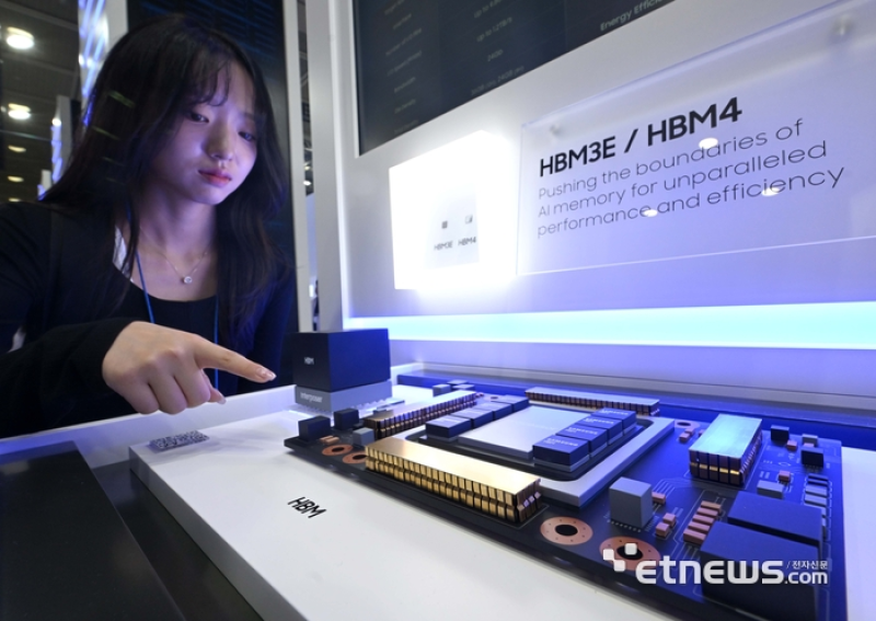
⬤ The technical hurdles are massive. Moving from today's 12-HI HBM4 to 16-HI means slicing wafer thickness from around 50 micrometers down to roughly 30 micrometers—while keeping total stack height at 775㎛ per JEDEC standards. That's like trying to fit more floors into a building without making it taller. It'll require bleeding-edge wafer processing techniques and brand-new manufacturing equipment that doesn't even exist yet.
⬤ The bonding process is another nightmare. Stacking DRAMs vertically means the glue holding everything together needs to get thinner with each additional layer. Samsung and Micron are betting on TC-NCF (Thermal Compression Non-Conductive Film), while SK Hynix is going with MR-MUF (Mass Reflow Molded Underfill). More layers mean trickier bonding and serious heat management issues to solve.
⬤ This competition's make-or-break for the future of high-performance memory. Whoever nails 16-HI HBM first won't just win Nvidia's business—they'll position themselves as the semiconductor industry leader for AI and other demanding applications. With computing demands exploding, the winner of this race could reshape the entire memory market.
 Victoria Bazir