Peter Smith

⬤ ASML and the broader semiconductor gear industry are watching lithography strategies closely, and there's a new data point worth noting. A recent chart breaks down how different manufacturing flows stack up across technology nodes from N+2 through N+6. Four approaches were compared: 2×SALELE+SALELE, 2×SADP+SALELE, 2×SALELE+SALELE+DFSAV, and 2×SADP+SALELE+DFSAV. The winner? The last one—Double Self-Aligned Double Patterning paired with SALELE and fully self-aligned vias—comes out as the most cost-effective option.
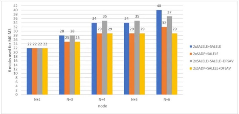
⬤ Here's what the numbers show. At the N+2 node, all four methods need 22 masks. But as you move to N+3 and beyond, the differences start adding up. At N+3, the Double SADP+SALELE+DFSAV flow uses just 25 masks versus 28 for the 2×SALELE+SALELE approach. Jump to N+4 and N+5, and the SADP-based DFSAV method holds steady at 29 masks while competitors climb to 34-35. By N+6, the gap gets even wider: 29 masks for Double SADP + SALELE + DFSAV compared to 32-40 for everything else. The takeaway is clear—as chips get more complex, cutting down on masks matters more and more for fabs running ASML lithography tools.
⬤ Why does this matter? Mask count is one of the biggest cost drivers in advanced chipmaking. Fewer masks mean fewer lithography cycles, simpler patterning, and lower manufacturing overhead. For ASML and the companies buying its equipment, that translates directly into better margins, smarter capital spending, and a clearer path forward as chips keep shrinking.
 Peter Smith